Direct Imaging of Stress in Crystalline Silicon Modules
As a DuraMAT project, Arizona State University (ASU) uses a laboratory-based, X-ray technique as a non-destructive and reliable way to monitor the deflection and stress as a function of materials, processing, and external stressors (loads and aging) on crystalline silicon photovoltaic (PV) modules.
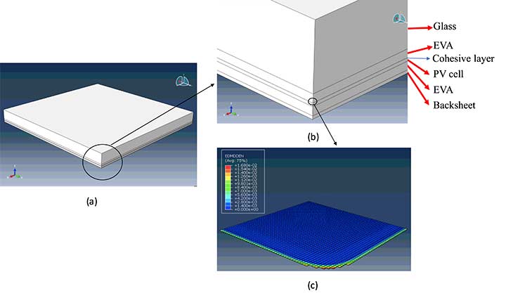
Cracking and micro defects are a significant cause of power losses and reduction in the levelized cost of electricity (LCOE). Applied stresses from the soldering and lamination processes promote the formation and propagation of micro-cracks. This increases the sensitivity of the system performance to shading and other failures. Therefore, ASU proposes that the process of module assembly today is optimized from the point of view of the inactive materials (e.g., encapsulant cross-linking), offering no insights into the solar cell status.
Core Objective
Location
Arizona State University
Applications
Models can be built to predict failure and optimize materials by understanding how deflection and stresses are distributed throughout the encapsulated cell, and how they evolve with aging and accelerated testing.
Availability
For information about the project's availability, contact Mariana Bertoni.
References
Xiaodong, M.; Stuckelberger, M.; Ding, L.; West, B.; Jeffries, A.; Bertoni, M. (2017). “Quantitative Mapping of Deflection and Stress on Encapsulated Silicon Solar Cells.” IEEE Journal of Photovoltaics. 8 (1): 189–95.
Contact
To learn more about this project, contact Mariana Bertoni.